An Arduino frequency counter

An Arduino frequency counter by WA5BDU


Introduction

This is going to be a fairly long description of the frequency counter and the ICs and circuits that make it go. That’s for people who might want to roll their own or modify this one. Otherwise, if you’re mainly interested in building one, gloss over all those details and just focus on the schematic diagram and source code.


A few years ago I wanted to design and program a frequency counter that could be embedded in a transceiver and output the frequency in Morse. I’d mostly moved from the PIC to the Arduino but I learned that the Arduino’s ATMega family of AVR microcontrollers could not perform high speed frequency counting directly like the PIC can. The PIC12F683 that I used has a prescaler front end that runs independently of its internal clock and can capture counts at over 100 MHz and as high as 140 MHz in my experience. It’s described in my blog linked below:


http://wa5bdu.blogspot.com/2017/11/pic-frequency-counter-with-morse-output.html


While doing my homework for that project, I got a  suggestion from one ham that I try the 74LV8154 32‑bit counter as a front end for an Arduino. It looked interesting so I took note.

My current need or at least my desire, was to design another frequency counter that could output readings at regular intervals to a serial port so they could be captured in a .CSV or other data array format and plotted. This was to plot drift and detect sudden jumps in frequency in the VFO of an old boatanchor I’ve been working on.


The 74LV8154 32-bit counter


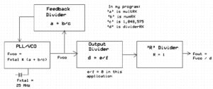
This is a great chip for this purpose. It has a 32 bit counter so it can go to 4.29E9 before rolling over. The 32 bit number is read  from four registers using 8 dedicated pins. Selection of which of the four registers to put on the pins is made using four dedicated pins, GAL, GAU, GBL, GBU, meaning A-lower, A-upper, B-lower, B-upper. (The counter can be divided into two 16-bit counters ‘A’ and ‘B’ but here we use them as one big 32-bit counter.)

Counting proceeds when –CCLR is HIGH and stops with counts cleared to zero when it is LOW. So the task is to make –CCLR HIGH for a precise amount of time (about 1 second in this case) and read the count at the end.

The internal count is transferred to the four output registers by a high to low transition on the RCLK pin. Timing of this action is important as we’ll see.

For the 32-bit counter, pins 1 (CLKA) and 2 (CLKB) are tied together and the signal to be counted is connected there. The chip is being operated at 5 VDC supply voltage, so the input signal should be approximately at the TTL level.

The data sheet doesn’t give the maximum frequency in direct terms, but I’m counting 50.125 MHz on it.


The HEF4521B, 24 stage divider with crystal oscillator


This is the chip that generates the approximately 1 second timebase signal. I actually made a version at first that didn’t use an external crystal timebase but instead let the Arduino generate it with a timer interrupt. It worked pretty well but had about 5 to 10 Hz of wobble in the last digit when measuring a 7 MHz signal. I wanted to get better stability.

I considered using a 32,768 Hz crystal such as are used in clocks and watches, but I didn’t think that could give the stability I wanted. I chose a 4.096 MHz crystal from my parts bin. It’s not an exact power of 2, so I don’t get an exact 1 second timebase but that’s fine as the actual value is accommodated in software. I need a 0.5 Hz signal to give the 1 second high time. The Q23 output on pin 15 does that, since 2^23 is 8,388,608. This gives me a 0.48828 Hz output with a period of 2.048 seconds and a high time of 1.024 second.

The data sheet gives component values for 50 kHz and 500 kHz crystals. I wasn’t sure if it could go to 4 MHz and did have difficulty until I noticed that in addition to Vdd and Vss pins, there are also Vdd1 and Vss1 pins that need power. No power, no oscillation. I stuck with the recommended values for resistors and capacitors except for making the the series resistor 3k3 Ω instead of 47 kΩ recommended for 500 kHz.

Not much else to say about this chip. It gives a lot of flexibility for your choice of crystal by having outputs for Q18 through Q24.


Logic and putting it together


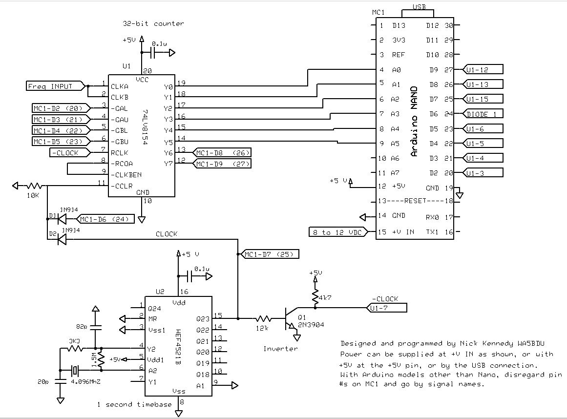
The basic idea is pretty simple. Connect the 1 second timebase clock to –CCLR so the chip will do a ~1 second count while it is high, then transfer the count to the output registers and read them into the Arduino, assemble and do arithmetic, essentially dividing the number of counts by the time of the timebase to give frequency.

There are a couple of complications, naturally. I’d like the end of the counting period to activate RCLK which will transfer the count to the registers. But this takes a low to high transition and at the end of the counting period, the clock is going from high to low. I hoped to avoid adding any more ICs to do miscellaneous functions, no NAND, NOR or inverter packages if possible. So I used a single transistor as an inverter, which you see in the schematic. Its output is –CLOCK or “NOT CLOCK”, being 180 degrees out of phase from CLOCK and it is used to trigger RCLK.

The next complication is with the signal to –CCLR. It goes low at the end of the counting period, which triggers RCLK, but it also clears the count in the same instant. So I have a potential timing race: Will RCLK cause the count to be latched to the registers before the simultaneous –CCLR clears it to zero? I don’t know the answer, but I didn’t want to leave it to chance.

To deal with this, I have the Arduino delay the low signal to –CCLR with one of its I/O lines. But I don’t want any software latency at the other end, where –CCLR is taken high, so I want the signal to be “armed” before that transition arrives. That’s the function of the two diodes, which I guess you’d call a negative logic AND gate. Both signals must be low for a low level to reach –CCCR.

The Arduino also needs to know when to enable and when to block the clear signal. So another I/O line monitors the clock signal. There’s plenty of time during each half cycle for it to do its thing. During the positive half, it raises the output signal to block the clear. After the signal has gone low, -CLOCK has triggered RCLK and the output signal can be take low to clear the count and allow the CLOCK signal to start counting at the transition to high.

I hope that all made sense.

The single IC version

In this version the HEF4521B and associated components plus the inverter are omitted and the clock and latch signals are provided by the Arduino. I’m posting a separate source code for this version since it works well enough to be useful and simplifies the hardware.  Arduino I/O line D6 goes to the RCLK pin and line D7 goes to –CCLR.

Displaying the output

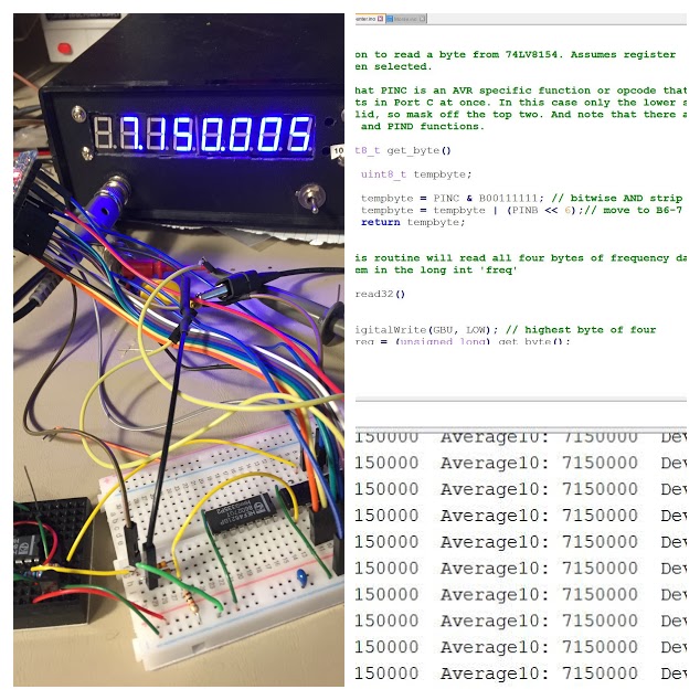
Since my original intent was to capture data over time for plotting, I’m printing the frequency to the serial port on one second intervals. Note that on the Arduino, you can turn on a serial monitor by pressing Control-Shift-M and see this output. On the version without the crystal timebase I was trying to quantify the amount of ‘jitter’ I get from software uncertainties. I wanted the deviation from average, not from some absolute value, so I keep a running average of the last ten counts and display each reading’s deviation from that average.  Here it is now looking at a 50.125 MHz signal:

frequency: 50124948  Average10: 50124948  Deviation: 0

So this is pretty solid. Usually there’s at least a bobble in the Hertz digit.

Here’s an output taken for the version with timing taken from the Arduino, looking at a 7.150 MHz signal:

frequency: 7149968  Average10: 7149966  Deviation: 6
frequency: 7149965  Average10: 7149967  Deviation: 1
frequency: 7149967  Average10: 7149967  Deviation: -2
frequency: 7149965  Average10: 7149967  Deviation: 0
frequency: 7149972  Average10: 7149966  Deviation: -1
frequency: 7149968  Average10: 7149967  Deviation: 5

I presume that at 50 MHz the deviations would have been about seven times as great. So … this was not bad but the addition of the crystal timebase was worthwhile.

Other incomplete things:

I: Other output options

An LCD or other display independent of a PC or serial monitor would be an obvious addition to consider.

I think my first move in this direction would be to add output in Morse, like the AFA (Audible Frequency Annunciation) type output of my PIC counter. I’d want a pushbutton to tell the Arduino when to speak up. I’m close to having this working.

II:  Other time base and calibration options

The one second time base is good as it gets you 1 Hz resolution. But a 0.1 second measurement would be good too as it would update ten times as fast. Since I’m dealing with powers of two, I’ll probably go with a 1/8 second measurement. Then I just multiply my counts by eight and process as usual.

Also, wasting one second for every second spent measuring isn’t good. I’m sure there’s going to be a way to reset and restart the time base so that the time between measurement periods is kept to a minimum.

 As for calibration, right now my method is pretty crude. I measure a known frequency with no correction, then take a ratio of the reading to the actual frequency and use that to correct the measuerement. It works, but having to revise my source code if things change isn’t good. I haven’t yet tried a trimmer on the crystal to see if I can tweak it in. Doing the software thing once and then tweaking a trimmer thereafter would be a good approach.

Also though, my adjustment math in software requires me to use floating point math. The numbers are just too big even for unsigned long integer math. But floating point limits the resolution to something above one part in 1E7. A good solution would be to have a crystal that will divide down to exactly 1 second, with a trimmer. Then I could avoid the software math corrections entirely. Update: I’ve got some 4.194304 MHz crystals on order that should do the job.

IV:  Input signal conditioning and amplifying.

Currently I’m using the counter with input signals of at least a couple of volts p-p at the input.  Some sort of amplifier plus limiter/squarer is normally used to increase sensitivity. The one from my PIC counter made from a single NAND gate gave me sensitivity in the range of 35 mVpp to 180 mVpp. Take one section of a 74HC00 NAND gate package. With one gate, tie the inputs together and feed them through a 0.1 uF capacitor. Connect a 22 k-ohm resistor from output to input. This is a simple solution that works great.

Link to source code for version with the crystal time base:

http://www.wa5bdu.com/wp-content/uploads/2021/01/Freq_counter_xtal.ino

Link to source code for a simpler version where the Arduino provides the time base:

http://www.wa5bdu.com/wp-content/uploads/2021/01/Freq_counter.ino

Link to the schematic diagram:

http://www.wa5bdu.com/wp-content/uploads/2021/01/Schematic-snip-frequency-counter-1.jpg

Programming the Si5351a synthesizer

 
What is being discussed here


I’m going to discuss how a program, or my Arduino program specifically, calculates register values for the Si5351a to put it on a specific frequency. I’m not going into details of how the register values are formatted into bit fields and actually sent to the chip via I2C.


Acknowledgements and sources


I’m not sure exactly which sources I borrowed pieces of code from. I took bits from libraries or programs and changed a few things. I know the method of producing quadrature output came from Hans Summers, G0UPL, and some of the basic calculation of register values did as well. A lot of what I’ve done here is to simply “reverse engineer” the code to see what it’s doing.

https://www.rfzero.net/tutorials/si5351a/ provides a nice overview of the chip and programming process.

Silicon Labs AN619 is a first resource. Some clarifications and corrections are provided by the page above and Hans Summers’ writings.


First, what is available in the component?


Below is a diagram of the Si5351a’s sections and functions


The Si5351a starts with a PLL/VCO loop. (There are two on the chip but I’m discussing one of them.) This loop adjusts the output frequency of the VCO such that it is an exact multiple of a reference crystal frequency. The program enters a divider number of the form ‘a + b/c’ to this loop and the logic divides the VCO output down to equal the crystal frequency. Put another way, you could say the crystal frequency is multiplied by ‘a + b/c’ to give the VCO output. Typical crystal frequencies are 25 MHz and 27 MHz.  Mine is 25 MHz. The data sheet calls the ‘a + b/c’ divider the Feedback Multisynth Divider, because it is in the feedback loop of the PLL/VCO.

The VCO output should be in the range of 600 MHz to 900 MHz per the data sheet. It will work reliably down to 400 MHz though. This limited range dictates the first step in selecting a divider number, however.  

Note that in the ‘a + b/c’ number, the value of c can be as large as 2^20 – 1 or 1,048,575. That means the VCO frequency can be set to fairly high resolution and in fact this is where we will adjust the frequency to give about 1 Hz resolution on the ham bands. The total of a + b/c can range from 15 to 90.

Following the VCO is another divider stage that divides the VCO frequency by a value of ‘d + e/f’ and can be used to take the frequency down into the low MHz range. However the chip will provide an output with lower jitter if this value is an integer and better still if it is an even integer. So we let e/f be zero and select a value for d that’s an even number. Remember that there is enough resolution in the PLL/VCO stage to provide fine tuning. This approach also simplifies the calculations required and speeds things up. The data sheet calls the ‘d + e/f’ divider the Output Multisynth Divider, because it acts on the output of the PLL/VCO.

I said the previous step allows reaching the low MHz range. If it is desired to go down into the kHz range, there is one more divider called R that can be used for this. R can be set to integer values 1, 2, 4, 8 … 128. In our example R =1 and so this stage has no effect on the output frequency.

Note that we’re down to six values to calculate which are the ‘a, b, c, d, e and f’ of the dividers ‘a + b/c’ and ‘d + e/f’. But it will actually be a lot simpler. We said that the second divider d + e/f will be an even integer, so e and f are not needed. Then in the first divider a + b/c, we will make c a constant so we are now down to three required values: a, b and d.


Method:


Our inputs are the desired output frequency Fout and reference crystal frequency Fxtal.

Recall that the second divider is to be an even integer. Known as ‘d’ above, it’s called dividerRX in my program. The output frequency of the Si5351a is the VCO frequency Fvco divided by dividerRX or

1)      Fout = Fvco/dividerRX

From practical constraints, a value of 126 is a first approximation for dividerRX.  To see if that value will work and keep the VCO frequency below 900 MHz, rearrange the above to give

2)      Fvco = Fout * dividerRX

The program performs this multiplication and checks on whether the result is > 900 MHz. If it is not, then dividerRX will be 126. If the result is > 900 MHz, a better (smaller) value for dividerRX is determined by rearranging the equation again and using 900 MHz as the target approximate VCO frequency so

3)      dividerRX = 900E6 / Fout

The remainder is truncated. Then the resulting integer is checked for odd or even. If it is odd, it is decremented by one to produce the final value for dividerRX.

Now we have a final value for dividerRX and can use equation (2) to calculate the exact value of Fvco required.

Having that value, we move to the PLL/VCO stage and calculate the required value of ‘a + b/c’. First the total value is calculated and then the individual terms are extracted to be sent to the Si5351a.

4)      Fvco = Fxtal * (a + b/c), or rearrange to

5)      (a + b/c) = Fvco / Fxtal

Equation (5) will give me a floating point number which is an integer plus a decimal fractional part. Truncating the number to just the integer gives me the value of ‘a’ which I call multRX.

Next I need to take the fractional part (remainder) of the result of equation (5) and use it to calculate b.  Call it ‘frac’. I need a ratio b/c that equals that fractional part. I’m allowed to choose any (almost) b and c that will give the best accuracy, but for efficiency I’ll make the denominator ‘c’ be the largest value allowed, which is 2^20 – 1 or 1,048,575. This will allow the finest resolution.  (More about that later.) From this I’ll calculate the value of b which in my program is called numRX.

6)      numRX = frac * 1,048,575

I drop any fractional part of that result and now I have an integer which is numRX, a.k.a. ‘b’.

Now it’s just a matter of sending the three values I’ve calculated to the Si5351a. It’s never exactly that simple though, as the values must be formatted in specific ways I won’t go into here.

What about quadrature?  There are registers in the Si5351a for phase offset called CLK0_PHOFF,  CLK1_PHOFF and CLK02_PHOFF for the three outputs.  Clocks 0 and 1 can be derived from the same PLL/VCO output so we use them. The method is to leave the clock 1 phase as-is (zero) and write the value of dividerRX to CLK0_PHOFF. This produces the 90° offset between the two.

I have a spreadsheet that will calculate the values produced by the program for any frequency, so to demonstrate the output for various desired values of Fout and a crystal frequency of 25 MHz, I have the table below.


To verify or see what these numbers do, divide Fvco by dividerRX and you’ll get Fout.

Next take multRX plus numRX / 1,048,575 and mulitply that times crystal frequency 25,000,000 and you’ll get Fvco.

Note that below about 7.15 MHz the default dividerRX of 126 is used and Fvco falls out where it will. Above that frequency, smaller values of dividerRX must be used to prevent Fvco from exceeding 900 MHz.


About fixing the denominator of b/c at 2^20 – 1


Doing this simplifies things and gives the fraction a resolution of about one part per million. However, there are sometimes values of b/c using a smaller denominator that would give a greater accuracy in approximating the desired value. Consider 1/4 for example. It can be expressed as 262,144/1,048,575, but that’s not exactly one-fourth. It’s actually 0.250000238. So you can see why we say “close enough”.

There’s an algorithm for calculating the best b/c for a number with the maximum value of c specified. It’s called the Farey Algorithm. I wrote (actually, translated) a C program to do it but it was too long to include in the Si5351a VFO. That is, it takes longer to execute than my desired program speed requires. So I stay with the quick and dirty method.


Go to my Si5351a quadrature page to see my source code:


http://www.wa5bdu.com/si5351a-quadrature-vfo/

An Arduino Si5351a quadrature VFO controller

Front view of the VFO. The display is indicating the Receive and Transmit frequencies, the step size, and the current mode. Pushbuttons PB1, PB2 and PB3 are surface mount type soldered to a bit of circuit board material.
 

Here’s a full-featured VFO I built around the Si5351a synthesizer IC and an Arduino controller. I’ve written a manual describing its construction and features and I’ll excerpt bits of it below as a description. I’ll also link to the complete manual as well as the source code. It’s painfully obvious that I don’t know how to use this HTML editor, so please forgive the strange formatting changes and misaligned bits.

Nick Kennedy, WA5BDU

After getting the basic functions working I began to expand my software to add features necessary to meet my needs for a VFO to be used in a transceiver project. Those features include:

  •  A keyed line input, so the controller can swap between TX and RX frequency outputs as required as the user keys and un-keys the transmitter.
  •  A TX_Out output pin echoes the keyed line input, but doesn’t change state until the TX frequency registers have been sent, and changes back to key up before the RX frequency registers are sent.
  •   An LCD display to show the frequency I’m on, menu options and so on.
  •  A user settable CW Pitch value which is the amount that the VFO shifts between TX and RX states if in CW mode.
  •  CW/Phone mode selection which functions to enable or disable the CW offset shift when the key line is closed.
  •  LSB/USB selection. This chooses the direction of CW offset in CW mode, so the user can listen to a station on either side of zero beat. In CW it’s sometimes called NORMAL and REVERSE operation. There is also an output pin SB_Relay than can be used control a sideband select relay in the receiver. As of V1.7, this function also changes the phase relationship between the two outputs from 90 to 270 degrees, so you don’t have to do sideband switching in the hardware.
  •  RIT control. This provides for separate TX and RX frequencies, with both displayed. The receiver can be tuned without disturbing the transmit frequency. RX and TX frequencies can be swapped and the offset can be zeroed without turning off RIT.
  •   Frequency step selection. There are both a menu for selecting from seven step sizes and a quick pushbutton selected step change between fine (10 Hz) and fast (100 Hz).
  •  Band selection with all ham bands from 3.5 to 144 MHz selectable.
  •  A Save State menu option which writes most of the current parameters into EEPROM so the VFO will start in the same state the next time it is powered on.
  •  Three miniature pushbuttons allow quick selection of often used functions while a menu controlled by the rotary encoder is used to access other functions. The pushbuttons operate with the familiar TAP and HOLD logic, giving two uses for each.
  •   A sidetone which sounds when the key is closed. A menu option can enable or defeat this function.
  • Optional third output with the transmit signal being on clock 2 and receive on clocks 0 and 1 (V1.14)
  • When the above option is used, clocks 0 and 1 can be keyed (off in transmit) for muting (V1.14)
  • For superheterodyne receivers, an intermediate frequency (I.F.) can be specified. It will be added to the displayed frequency (V1.14)
  • Optional x4 output, for receivers using a flip-flop to develop quadrature signals (V1.14)
  • Option of using an LCD display with the standard parallel interface, or one using an I2C interface (V1.14)
  • A single output on clock 0 can be used instead of quadrature on clocks 0 and 1 (V1.14)
  • Setting number of pulses per step, to tame high speed rotary encoders (V1.14)

Details of operation

The pushbuttons offer six actions, one of which opens a menu with additional actions. A brief press of a pushbutton is called a TAP and a long press (> 0.5 second) is a HOLD operation.

There is audio feedback in the form of a short beep immediately as a switch is closed, followed by two short beeps after it has been held long enough for the HOLD function.

 
Above is a listing of functions accessed via the pushbuttons. I tape a copy to the top of my VFO for reference.

There’s a great deal of detail to discuss concerning use of the functions of the VFO, but I’m going to refer the interested reader to the manual and try to keep the size of this page down. I do want to tell a bit about the hardware.

Hardware requirements:
  • An Arduino board, such as a Nano or Uno

  • A Si5351a module

  • A rotary encoder

  • A standard 16×2 LCD display with Hitachi parallel or I2C interface

  • Three N.O. pushbuttons

  • A few miscellaneous diodes, resistors capacitors and connectors

An Arduino might be $4 to $5 for a Nano or $9 or so for a Uno

A Si5351a module might be $5 or so. I like the module over the bare chip for avoiding difficult soldering and because it has a built in 3.3 V regulator and 5 to 3 volt logic level shifters for the data lines. You can power and talk to it from your 5 V Arduino.

My rotary encoder is a Bourns PEC11L-4020F-S0020 encoder with switch from Mouser.  The switch isn’t used. Update: I’m switching to an optical encoder as these inexpensive mechanical ones do wear out and give erratic performance after a time. 


Below is a schematic for the VFO.   The USB/LSB select relay if used would be driven by A2. Connection options for LCD with parallel or I2C interface are shown.


Here’s a photo of the rear of the VFO. CLK0 and CLK1 are the two quadrature RF outputs.  The KEY/PTT input will cause the VFO to swap between receive and transmit frequencies, it will also generate a sidetone if desired and actuate a Key Out circuit with which to key a transmitter.
 

Above is a photo of a Si5351a module connected to an Arduino UNO for testing. I think it’s impressive that with just four wires the system functions by coming up on the default frequency with quadrature outputs.
 

Here’s an oscilloscope trace of the two quadrature outputs. The output is about 3 Vpp open circuit and about 2.1 Vpp into 50 ohms.
 
A couple of variations

Some receivers have a divide-by-four logic arrangement in front of a circuit that develops I & Q signals. Since this VFO provides I & Q outputs already, there’s generally no need for an output of four times the indicated frequency. However, one friend wanted to use this VFO with his existing hardware which needed the X4 signal. So I added a flag which will cause the VFO to operate in the X4 mode. It requires editing one line in the source code. At startup, the LCD reminds you of which mode is being used.

The Si5351a can have up to three outputs. Friend #2 wanted to use that 3rd output to drive his transmitter while the other two were used for his phasing receiver.  There’s no reason you couldn’t use one of the two quadrature outputs for the transmitter, since it already jumps between TX and RX frequencies. But my friend didn’t want to risk adverse loading effects by having both a RX and a TX stage driven off the same output.  So I did another version which provides a third output on CLK2 for the transmitter. After some comedy of errors keeping it on the right frequency and making sure it didn’t QRM the receiver, I think I finally got it right.  


Changes made in V1.8, released January 20, 2023   (also, V1.9)

I sometimes get feedback from users with fast rotary encoders, meaning they output a lot of pulses per revolution. This can cause the pulses to outrun the software leading to erratic stepping. I decided to change the input signal processing from a polling method to interrupt driven. Making this change required changing Arduino pin usage such that two pairs of wires need to swap places. Don’t install V1.8 if you don’t want to make these changes. They’re described in the manual. 

The interrupt code accumulates step demand pulses in a queue and the main line code works them off as fast as it can. To speed things up, if the queue contains 10 or more demands, it increases the step size by a factor of 10 and does 10 demands in one pulse. 

Some encoders can be very fast, making tuning too sensitive. Another change in V1.8 allows the user to compile the software to give one step per pulse, one step per two pulses, or one step for four pulses. (Now V1.9 allows any value from 1 to 255 as pulses per step.)

Variations in encoders have caused most of the problems reported to me. My own mechanical encoder has become pretty noisy. I’m hoping that switching to an optical encoder will smooth things out. 

I also developed an Arduino program to allow troubleshooting encoder problems. It uses a separate Arduino to generate simulated Arduino pulse trains of varying length and direction and repetition rate. This is mainly to insure a clean pulse train when testing flaky software. Also it can be used to find out how fast the utilization software can process pulses. I may put it on line but if you are interested, email and I’ll send you the sketch and a manual of sorts in Word format.


Changes made in V1.7, released April 29, 2022

I fixed a few bugs you’ll see reported in the comments section, most of which were fairly minor. One more serious bug caused the 90  degree phase offset between the two outputs to be lost, ruining the quadrature relationship. This would occur while adjusting the frequency and crossing a certain threshold, such as going from 7142 kHz to 7143 kHz. That problem has been diagnosed and corrected. Thanks Tony Bertezzolo, IZ3EYY.

Also in some cases, enabling the RIT resulted in the RX and TX outputs being in different bands. Also corrected.

There’s also a new feature. A software switch now allows changing the phase difference from 90 degrees to 270 degrees. The existing control for selecting USB or LSB (tap PB3) will cause this toggle. The advantage is that you won’t have to design upper and lower sideband selection in your hardware – it’s now in the VFO.

Files you’ll want:

Links to the manual for the VFO and for the Arduino source code are given below. The manual is a PDF file. It includes information on processing the source code in the Arduino IDE and sending it to your Arduino. The file ‘si5351a_quad.ino’ is the Arduino source code, which is a plain text file. As of V1.14, there’s also a “config” header file which goes with the main source code file.

Si5351a_VFO_manual

si5351a_quad

si5351a_quad_config

wa5bdu-home

Some pages of projects or technical information


Links to pages for projects and info:


ContentsLink
An Arduino and SI5351a VFO projecthttp://www.wa5bdu.com/si5351a-quadrature-vfo/
Calculating register values for the Si5351ahttp://www.wa5bdu.com/programming-the-si5351a-synthesizer/
The WA5BDU Keyer for the Arduinohttp://www.wa5bdu.com/the-wa5bdu-keyer/